USB Type C super-speed routing doubts

USB Type C super-speed routing doubts

Anonymous
Not applicable
19,373 Views
45 Replies
Message 1 of 46

USB Type C super-speed routing doubts

Anonymous
Not applicable

Hi All


I have designed a USB - USB type C receptacle pass-through board. I have started routing the 90R controlled impedance tracks for the USB. I've got the information from the manufacturer to use a trace width of 0.22mm and trace spacing of 0.125mm to achieve 90R impedance. I heard D1_P and D1_N needs to be short to enable the flipping feature. It is a four layer board. I am attaching the schematic and board layout.  Could anyone guide/help me with the layout? Is that correct?


Thanks

Accepted solutions (1)
19,374 Views
45 Replies
Replies (45)
Message 21 of 46

Anonymous
Not applicable

Also a couple of clarification 


As far as I've understood in a way that RODmodded2 is the good one to use and with modifications like 
1. vRestrict layer added to stop Via's
2. to double check with you as there is no need to place tRestrict layer right as there is no trace? but I am confused with the point that it removes Ground plane polygon pour. As I don't see a tRestrict layer on the board layout. 
 
Could you please clarify.
Thanks
0 Likes
Message 22 of 46

Anonymous
Not applicable

Hi Dhinesh

I don't get those errors here.
I am currently using version 9.1.2 of Eagle PCB?

What version of Eagle are you using?

Rod.


0 Likes
Message 23 of 46

Anonymous
Not applicable

You seem to have missed the point that this is a vRestrict OR tRestrict choice and not a vRestrict AND tRestrict (although possible)
The notes in the PCB design attempted to tell you:
1. that vRestrict (unusual) has been used for the PCB restriction area.

All this will do is serve to warn people if they inspect in detail the device/package footprint
And restrict Autorouting from working properly in this area (as it can't auto place vias)
You can still manually place them.

2. that tRestrict (more usual) has NOT been used for the PCB restriction area.

Primarily because it acts on the area under the connector metal to prevent track placement (we DO WANT this feature)
But also, in addition, it stops the ground plane polygon poor on that area (we actually DO <NOT> WANT this feature).

3. The choice, in either case, is not ideal but the use of 1. has been my preference, but may not be the best one for you (perhaps 2 is better), it depends on the circumstances and priorities.
Refer here for an explanation of the different layers functions.
http://dangerousprototypes.com/blog/2012/08/08/how-to-eagle-keepout-and-restrict-layers/
Hint (in case you did not notice - although your query 1. suggests you did):
v=via and t=track in vRestrict and tRestrict respectively.
Note: Multiple restrict layers can be added together to do something else (that is the nature of PCB layering).

4. That the restrict area SHOULD (not essential) be removed from the PCB layout and instead placed into the device library (which I would need you to email so I can do for you, if you don't know how.)

==============================================
The problem here is that Eagle PCB does not have a suitable Layer that does exactly what is needed (as far as I am aware) in this case and cannot easily be set up, to create one that does (it may be possible).

==============================================
PLEADING TO DEVELOPERS (If they are reading)
Please allow a device footprint (in the board) and label (in the schematic) to have message attribute (and/or layer) set that:
A. can be prompted at user placement in Schematic or Board respectively;

B. can somehow be used to advise a user of special issues when routing to a mRestrict area (i.e. m=message);

C. ideally allowing component designers to actually do a wider variety of restrictions (like in this case);
D. Or rather than using an attribute somehow linking a special Text note on perhaps the new Layer mRestrict (that appears in the PCB layout, but also displays to the user in a dialog box.  With a UI-option=on by default for each new PCB design.


Rachael (if she reads this), may have a better solution idea as her experience is greater than mine.
==============================================


Additional clarifying points to make:

5. None of the notes should come out in Gerber files (CAM process) as they are on documenting layers.

6. While you can delete the notes in the PCB, it may be important to leave them there, primarily for future editors (possibly not you); definitely delete the circles.
7. The PCB restricted area (currently set to vRestrict) has not been placed with super accuracy (as I was tired and in a rush - I have spent way too much time on this problem).

Message 24 of 46

Anonymous
Not applicable

@Anonymous wrote:

Hi Dhinesh

I don't get those errors here.
I am currently using version 9.1.2 of Eagle PCB?

What version of Eagle are you using?

Rod.


I said errors but they are actually WARNINGS only and not critical.  They look like they are DRC related so will possibly disappear if you do a new DRC and then save and re-open.

Message 25 of 46

Anonymous
Not applicable

I just had another thought regarding the horizontal USB connector prohibited are (i.e Restricted area):

Perhaps the best solution is to add a large SMT pad (same size and location as the datasheets shows) to the connector footprint that is assigned to GND in the Schematic, this way it stops the placement of tracks but allows GND vias without DRC errors.  And will join with or without (I would choose this option) thermal relief (as set in the footprint design).
It seems like an ideal way to solve all the issues and still restrict tracks from being used in that area.

If creating components is new to you send me the library file and I will fix it for you and also update the eagle layout etc.

Message 26 of 46

Anonymous
Not applicable

Rod

I think you are using the latest one 

but I am using version 7.7.0.

0 Likes
Message 27 of 46

Anonymous
Not applicable

Yes, that makes sense now. I didn't realise that is vRestrict OR tRestrict. 

Points: 1, 2,3 makes sense as well

4. Aww, so the restrict area should be implemented in the footprint. I can make it myself and double check with you through an email.

5. Yes, I will make sure that notes not appearing in the Gerber. 


Thank you so much for your precious time which gives me a broad knowledge of PCB. 


0 Likes
Message 28 of 46

Anonymous
Not applicable

This is also an excellent point. 

Good to implement. Probably I can do this myself. 


Much appreciated!!!!!!! 

0 Likes
Message 29 of 46

one-of-the-robs
Advisor
Advisor

@Anonymous wrote:
2. that tRestrict (more usual) has NOT been used for the PCB restriction area.

Primarily because it acts on the area under the connector metal to prevent track placement (we DO WANT this feature)
But also, in addition, it stops the ground plane polygon poor on that area (we actually DO <NOT> WANT this feature).

If you want to keep an area of board clear, use a tRestrict. If you want to always have a ground pad there, why not put an SMD pad there?


@Anonymous wrote:

Hint (in case you did not notice - although your query 1. suggests you did):
v=via and t=track in vRestrict and tRestrict respectively.


Actually, v=vertical (I think) and t=top. There's a bRestrict layer, too. Perhaps a bit pedantic but...


Message 30 of 46

one-of-the-robs
Advisor
Advisor

@Anonymous wrote:

Rod

I think you are using the latest one 

but I am using version 7.7.0.


That would explain the errors you saw on loading Rod's files. They are reporting that V7 does not understand some of the parameters and options that have been added in V9. They should be harmless as the unkown tags just get ignored.

Message 31 of 46

Anonymous
Not applicable

Thanks

Rod also mentioned putting SMD pad there.


I believe this is the correct oneI believe this is the correct one

0 Likes
Message 32 of 46

Anonymous
Not applicable

That's good then. I can ignore those warnings. 

0 Likes
Message 33 of 46

Anonymous
Not applicable

@Anonymous wrote:

I just had another thought regarding the horizontal USB connector prohibited are (i.e Restricted area):

Perhaps the best solution is to add a large SMT pad (same size and location as the datasheets shows) to the connector footprint that is assigned to GND in the Schematic, this way it stops the placement of tracks but allows GND vias without DRC errors.  And will join with or without (I would choose this option) thermal relief (as set in the footprint design).
It seems like an ideal way to solve all the issues and still restrict tracks from being used in that area.

If creating components is new to you send me the library file and I will fix it for you and also update the eagle layout etc.


Another point (final one I hope).  When creating the SMT pad for the restricted area...be sure to disable the Stop mask and so that the solder mask cover (rather than uncover) the copper in production.  I think by default a SMT pad will have the solder (stop) mask and paste masks on. So also disable the Paste mask as you will not want a huge section of solder paste either as the connector is held in with soldered posts anyway.

0 Likes
Message 34 of 46

Anonymous
Not applicable

Yeah, thanks for that heads up on that t=track error, when it actually means top (as I did know)...I don't want to confuse people.  I was just very tired when I did that (I am down under in Australia).  BTW I didn't know v = vertical though but makes sense too.  Tks, Rod.

0 Likes
Message 35 of 46

Anonymous
Not applicable

Thanks

I've emailed you with the changes. Please let me know if that is ok?

0 Likes
Message 36 of 46

Anonymous
Not applicable


Hmm.. Here I go again:

Dhinesh: The "solution" you have now will likely work it is not what I would do.  I finally have concluded a logical reason for the two symptoms you had in one direction on High Speed (USB2) and SuperSpeed (USB3).  And I believe it is the same issue with the connector restricted area being too close to the run tracks on that side of the connector.

Although, it is a little confusing that SuperSpeed (USB3) also did not work properly in one orientation of the Type-C connector (assuming it was checked).  Referring to these comments in an earlier reply.


@Anonymous wrote:

That original ("previous" i.e. failed) design you posted looks just like the way I would have run the USB2 lines i.e. D1_P & D1_N, with separate D2_P & D2_N also. As I was trying to describe in the previous reply. 


@Anonymous wrote:

Regarding D1_P, D1_N and D2_P, D2_N 

This is the previous connection used for both schematic and board layout but it is failed to work reverse. It was working only one side.

Besides, it appears from another of your comments that Superspeed failed altogether, which has NOTHING to do with the USB2 lines (i.e. they are not used in Superspeed mode).

@Anonymous wrote:

failed to work at super speed it is working at high speed 


Let me try to explain further:

The below image shows the new design that you created before I edited it, where the edge of the restricted area as explained earlier is likely creating a high frequency (RF) impedance short.  The edge of the restricted area of the horizontal USB3 connector shows three different pair problem areas - these explain all symptoms described!The edge of the restricted area of the horizontal USB3 connector shows three different pair problem areas - these explain all symptoms described!


These are essentially the same in the originally tested circuit illustrated by this image you posted earlier:


How the original design ran the USB2 lines and how I still believe they should be run.How the original design ran the USB2 lines and how I still believe they should be run.

So given that the original board failed to work at super speed and it did work at high speed but it is failed to work reverse.  You can see that these are consistent (if not complete)  with the three flawed track routings that edge up to the restricted area.  That is the two outside ones would cause the SuperSpeed (USB3) failure and the inner one would cause a USB2 failure in one direction as the pair on the other side would allow the High Speed (USB 2) to work properly, but in only one direction.


My Conclusion

So while it is possible the new "solution" will work I strongly believe the USB2 crossovers do not belong in the intermediary connector but should exist only as required at the host and device ends of the USB path. So I strongly believe that they need to be switched back to this form:

With corrections for the restricted area adjacent to the horizontal connector.With corrections for the restricted area adjacent to the horizontal connector.

Modified PCBModified PCBModified SchematicModified Schematic

I will email the changed files also.  Hopefully, you have not made many changes to it already.
If you find it hard to accept this design, at the very least, I strongly encourage you to get both boards made and test both designs.
Rod.

0 Likes
Message 37 of 46

Anonymous
Not applicable

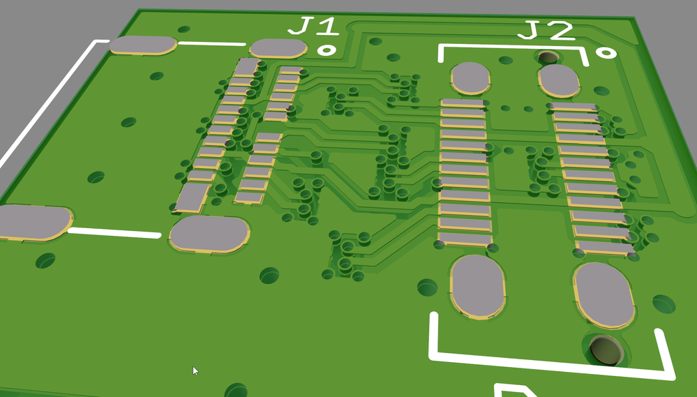
Using the excellent and free 3D viewer I use: https://www.zofzpcb.com/

TopTopBottomBottomDue to track congestion I had to run the CC2 (DC signalling only) on layer 2Due to track congestion I had to run the CC2 (DC signalling only) on layer 2

0 Likes
Message 38 of 46

Anonymous
Not applicable

Hi Rod

It's all done as per your advice. Please see email

Great, thanks

0 Likes
Message 39 of 46

Anonymous
Not applicable
Accepted solution

OK, I checked your final PCB layout (via email), and I just added in some grounding and made some slight alignment changes to allow more grounding around diff pairs.

These are marked by circles as usual (check both sides if you're looking for the changes).
To do so I had to change the default net track width to 0 to get some thinner GND tracks as needed to fit.
 
I also looked at the diff-pair track length differences and they all look pretty good.
The best way (I find) is to select the diff-pair net class and look at the list of nets in the properties area.
Here you can see the track lengths and via counts easily (they are also dynamic when making changes).
It is a much better approach than using the Meander option to compare.
 
Cheers, Rod.
Comparing diff-pair track lengths - the easier way!Comparing diff-pair track lengths - the easier way!
Message 40 of 46

Anonymous
Not applicable

Rod


 Are you sure the facility for checking the diff pairs length is working in V7? I don't see any list underneath.

0 Likes