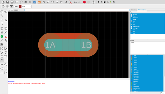
Slotted Pads

millingm
Enthusiast
Enthusiast

Slotted Pads

millingm
Enthusiast
Enthusiast

Has anyone got a good method for defining a slotted via/pad for those pesky connectors that need such a thing.  e.g. HDMI, vertical USB3 micro B, USB Type C. etc etc etc.


We've had several attempts and always had issues with either DRC or Gerber manufacturing data.  For example it's quite easy to define top and bottom copper and solder mask details but this doesn't put a restriction on where copper can flow (when using say a GND layer polygon) in the inner layers, unlike a Pad or Via does.


The Long round pad is almost correct but needs a method for defining a slot instead of a hole.   


Help? New feature? Please!!!


Reply
8,138 Views
37 Replies
Replies (37)

C.Nicks
Advisor
Advisor
Hi Millingm,
So far Eagle doesn't have a native way of defining a plated slot, but there are a few ways to get that information to the fabrication house.
I think the feature has been suggested before.

Essentially you'll want to use the long round pad to define the pads through the layers, then use a shape in the milling layer (46) to show the slot cutout. Then output the milling layer as it's own gerber with the instructions stating that it should be used for plated slots.

Check out https://forums.autodesk.com/t5/eagle-forum/custom-plated-oval-hole-for-usb-micro-b-connector/m-p/695...

Best Regards,
Cameron


Eagle Library Resources


Kudos are much appreciated if the information I have shared is helpful to you and/or others.
Did this resolve your issue? Please accept it "As a Solution" so others may benefit from it.

millingm
Enthusiast
Enthusiast

We have used your suggested approach but the clearance rules do not get passed onto the internal layers so we have had occasions where a slotted connecter pin ends up shorting to power planes on a multilayer board.  This clearance is something we need to define, not our PCB house.  It's a little different to saying plate these holes, do not plate these others.  We need a method to prevent copper with a different name flooding the area that is going to be machined and then plated on the inner layers.  


Perhaps an inner restrict layer might be a valid approach?


Our current preferred method is put a shape into the dimension layer (20) which will prevent polygons or wires going through the area to be machined but this raises so many DRC errors it's ridiculous.   Overlaying a load of pads is quite effective too, but it's messy and DRC error heavy too.


There are some many high density connectors coming out that need this it really needs to be addressed in future rather than spending time messing with the basic interface.


rachaelATWH4
Mentor
Mentor

@millingm wrote:


Perhaps an inner restrict layer might be a valid approach?


This was raised previously as a suggestion. I think the general consensus is it's a good idea so I think Jorge added it to the todo list.


@millingm wrote:


There are some many high density connectors coming out that need this it really needs to be addressed in future rather than spending time messing with the basic interface. 


To be fair to Autodesk they've done an awful lot more than just mess with the basic interface, especially in v8.3 and v8.4 so I think this is a little unfair.


I completely agree this should be addressed, it should have been long ago. Fortunately I haven't had to create many parts which require this but if more parts are starting to then it'll start to become a bigger issue if they don't get it fixed.


Best Regards,


Rachael


0 Likes

jorge_garcia
Autodesk
Autodesk
Hello Everyone,

I've added this thread to existing report for slotted pads.

Let me know if there's anything else I can do for you guys. Fully agreed this is something that needs to be addressed soon.

Best Regards,


Jorge Garcia
​Product Support Specialist for Fusion 360 and EAGLE

Kudos are much appreciated if the information I have shared is helpful to you and/or others.

Did this resolve your issue? Please accept it "As a Solution" so others may benefit from it.

_r_y_a_n
Participant
Participant


Hi Jorge,

How is this progressing? 

This feature is desperately needed. 


0 Likes

jorge_garcia
Autodesk
Autodesk
Hi @_r_y_a_n,

Thanks for following up. It's definitely being worked on, but implementing this in a general sense is a lot of work. It's high on the priority list. Stay tuned.

Best Regards,


Jorge Garcia
​Product Support Specialist for Fusion 360 and EAGLE

Kudos are much appreciated if the information I have shared is helpful to you and/or others.

Did this resolve your issue? Please accept it "As a Solution" so others may benefit from it.

Anonymous
Not applicable

Ciao Jorge,

it's only few days that i use Eagle and slots is a missing tool.

I'm glad if Eagle team make this; about Eagle, i like that it is a dinamic software and Eagle team is active to make improvements.


It will be usefull if there was a tool to draw custom pads, with particular forms, as like an offset pad with external square or exagonal form.


Thank you


Silvio

drey.platt
Explorer
Explorer

I’m very happy to find this feature is high on the priority list. I just switched our company to eagle premium only to discover how difficult it is to add a usb c connector which required a slotted hole! Still haven’t been able to finish and had to open circuitmaker to get the pcb designed. Really want to use eagle but missing a feature like this will be a make-it or break-it situation for us. 

millingm
Enthusiast
Enthusiast
We have always managed to find some kind of work around. E.g. A number (quite a few) through hole pads overlapping each other to create a rough slot. Put enough down so that the design rules force internal layers to be clear of the slot and simply have a word with your manufacturers and say the intention is to have a slot. No problems.
We have tried other things but you just have to check that any internal layers (particularly planes) do not get shorted when the slot is plated.
Note: you will get design rule errors.

Anonymous
Not applicable

Hello Eagle Team,


What is the progress for adding this feature?

This morning I lost 1 hour trying to figure out how to properly draw the footprint of a micro USB 2 connector (amphenol 10118194-0001LF).

I have come to the conclusion there is no perfect way of doing so...


Victor

0 Likes

rachaelATWH4
Mentor
Mentor

Hi Victor,


Unfortunately there is still no option for creating a plated slot in the library editor with the ease you can an SMD or PAD. However, you can do as @millingm suggested or the variation I prefer which is a PAD on each end of the slot and then draw each of the inner/outer layer pad areas with a polygon on each of the 16 routing layers. The also draw the slot as a line on the Milling layer. You end up with something like this in your library:


image.png


And when it is in the board you end up with:


image.png


It's a bit long winded to do for the first slot but when you've done it once you can group it and copy it for as many slots as you need in the footprint. You can see it works though, it correctly isolates polygons on all layers, object avoidance should keep other routes from it as you are routing and you can route correctly to it.


Finally, you'll need to add an indication in your build notes as to the intention for these slots and you must communicate this explicitly to your manufacturer to make sure they are aware of this and what they need to do.


Best Regards,


Rachael

millingm
Enthusiast
Enthusiast
The only reason I didn't do that was that you had to predict how many layers your board is. For a generic package that many engineers are going to use on any number of layers you would have to default to adding lots of layers in your package.
Given the fact that there are so many parts out there with odd shaped SMT pads or slotted details, Eagle needs to handle this without some lateral thinking required!
0 Likes

rachaelATWH4
Mentor
Mentor

@millingm wrote:

The only reason I didn't do that was that you had to predict how many layers your board is. For a generic package that many engineers are going to use on any number of layers you would have to default to adding lots of layers in your package.


In my above example I created it in the library with the polygons on all the routing layers. In my board it only brings it into active routing layers, in the case of the example it's a 4 layer board so I only need to create it once and don't need to predict layer usage in advance. Having the extra layers in the package doesn't seem to create any issues as far as I can tell.


@millingm wrote:

Given the fact that there are so many parts out there with odd shaped SMT pads or slotted details, Eagle needs to handle this without some lateral thinking required!


Oh, I completely agree, EAGLE really does need to get proper support for this added, we are on the same page here 🙂


Best Regards,


Rachael

0 Likes

jartza
Participant
Participant

I don't quite see how hard this has been to implement to Eagle. As a simplest thing you need a tool to select start and stop coordinates, other parameters being the same as regular through-hole pad. Then practically you just create polygon for pad a slot. In Gerber generation, G85 has been supported by PCB houses for a decade.

This has been requested to Eagle for years, and while I agree it must be some work, it definitely would have been implemented already if there was any will for it, but I guess all the 3D-features and other eye-candy is more important than productivity.

For us, this has become showstopper for Eagle, and we decided not to continue the subscription, and started converting the projects to other EDA tool 😞

rachaelATWH4
Mentor
Mentor

@jartza wrote:

I don't quite see how hard this has been to implement to Eagle. As a simplest thing you need a tool to select start and stop coordinates, other parameters being the same as regular through-hole pad. Then practically you just create polygon for pad a slot. In Gerber generation, G85 has been supported by PCB houses for a decade.


Yeah, I think I probably have to agree here. I really can't see it being so hard to implement.


@jartza wrote:


This has been requested to Eagle for years, and while I agree it must be some work, it definitely would have been implemented already if there was any will for it, but I guess all the 3D-features and other eye-candy is more important than productivity.


I think there is a will for it, but EAGLE was starved of resources for many years and there was a long list of stuff that people were shouting about, a lot of which have actually been implemented! They've done a lot more than eye candy, the Fusion 360 integration is actually functionally very useful, but apart from that how about all the routing changes?


@jartza wrote:


For us, this has become showstopper for Eagle, and we decided not to continue the subscription, and started converting the projects to other EDA tool 😞


Do none of the solutions above help with this? I know it's a bit of a fiddle but I've done quite a few parts with slots now and it does work so it's not been a show stopper issue for me, just a bit annoying.


Best Regards,


Rachael

0 Likes

millingm
Enthusiast
Enthusiast
It's the kind of annoying thing that if not done right can cost a lot of time and money to resolve.
There is no formal documentation or guidance on how to do it either. Needs sorting - long overdue.

rachaelATWH4
Mentor
Mentor

@millingm wrote:

It's the kind of annoying thing that if not done right can cost a lot of time and money to resolve.


Absolutely. I almost had a disaster when I first tried to do this but an on the ball PCB vendor spotted the issue. I now have added items to my release checklist to make sure I thoroughly check any slots to ensure it's correct and my process for this is now robust (but still annoying!).


@millingm wrote:

There is no formal documentation or guidance on how to do it either. 


You are right, it's all on forum posts mainly. The workarounds should be written up in detail somewhere official and also either included in or referenced from the built in help.


@millingm wrote:

Needs sorting - long overdue.


I totally agree, fixing this is definitely long overdue. Hopefully they'll take note and get something sorted sooner rather than later.


My point from my previous message was that whilst it's a really glaring omission that most other tools deal with nicely now, if done right the workarounds do work and aren't (for me) show stoppers which prevent designs with plated slots being completed.


Best Regards,


Rachael

0 Likes

kadah.coba
Enthusiast
Enthusiast

2 years later and still nothing.... I'm regretting investing so much time in to learning Eagle as I spend more time trying to find and do these workaround than actually getting anything useful done. Its disappointing that new icons, more padded UI and less board view were a higher priority that something useful.

Anonymous
Not applicable

I just wanted to add in that I used Rachael's method for making slotted pads, and it took me all of 15 minutes to make three slots for a part I am using. It isn't as quick as it could be, but it works quite well. Thanks for sharing your method, Rachael.