@jprzezdziecki wrote:
Should I create two different (named) T092 packages for those devices? How this should be done. When I use the same TO92 package it conflicts with a second device with different pinouts (the connected pinouts are wrong).
I have checked with "transistor-fet.lbr" and 2N3819 and BF245 have different pinouts BUT they are connected to the same TO92 package.
I think @skndungu75TT4N3 misunderstood your question, or at least understood it differently to me, which isn't necessarily the same thing.
There is nothing to stop you associating the same package with multiple devices and no reason they can't have different pin-outs. Look at the TTL library, for example - many devices sharing the DIL14 package with totally unrelated pin-outs.
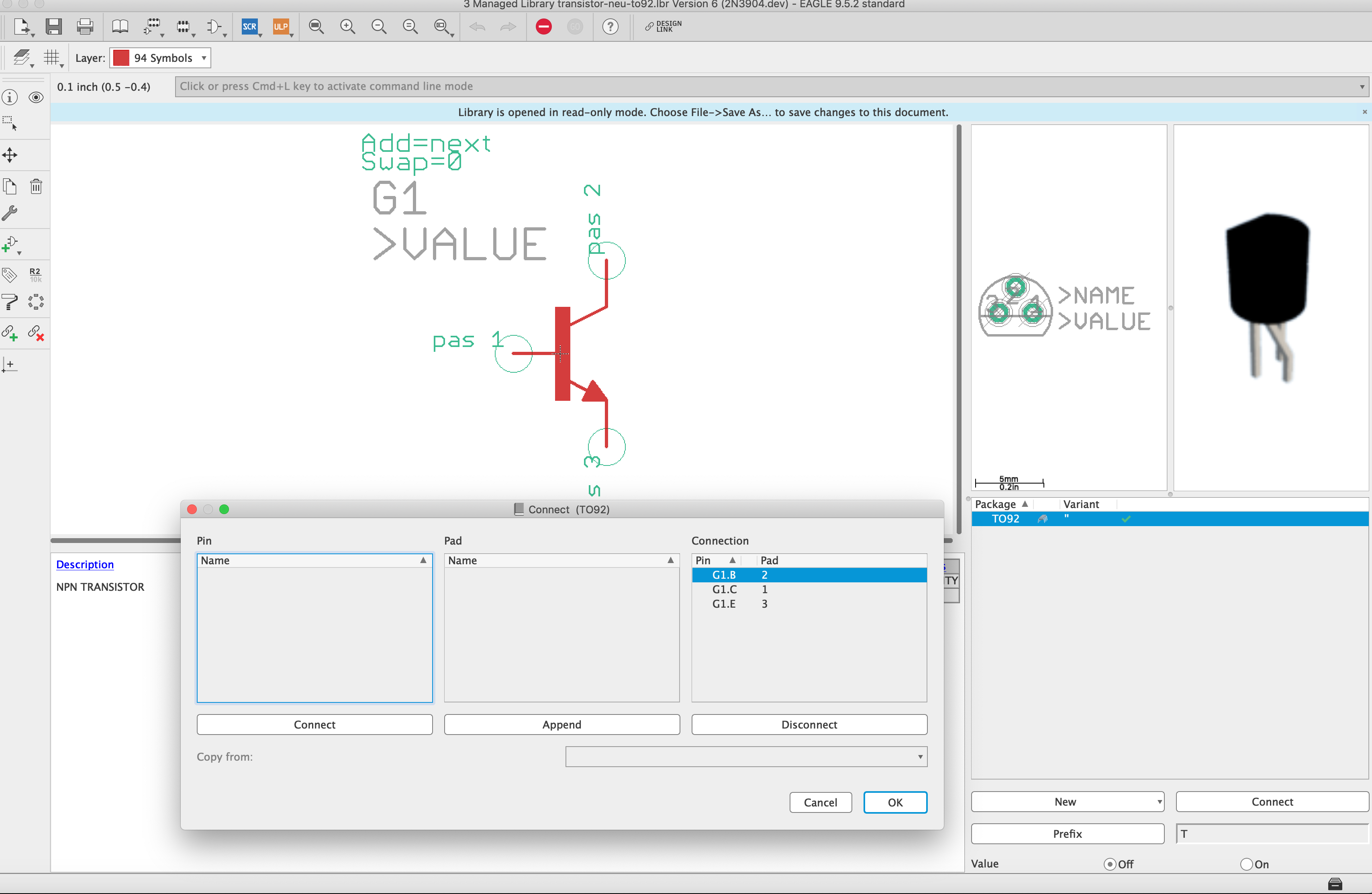
The schematic symbol has a set of "pins" with names that you assign when you create it. For a FET, these will typically be "G", "D" and "S".
The package has a number of "pads" with names that you assign when you create it. In most cases, the JEDEC or other appropriate spec. allocates plain numbers, "1", "2", etc., although sometimes there are special cases.
When you create a device, that device contains one or more symbols as "gates", and one or more packages associated with "variants". Since you name the variants, you can easily identify them. Within this association, you define a mapping from symbol pins to footprint pads.
There is nothing to stop you assigning the same package/footprint to multiple variants. If you do so, you can define different pin/pad mappings for different pin-outs.
There is one caveat. Although I said above that the footprint normally has simple numbers for the pads, some people draw footprints and give functional names to the pads. This is bad practice, especially if they have named TO-92 pads as "G", "D" and "S", because not only do some FETs have different pin-outs, but some (many!) TO-92 devices are not FETs. If your library has such a "customised" TO-92 footprint, you can still re-allocate the pin-out on your second device variant, but it gets confusing. It's better to rename the pads. Eagle will automatically adjust any devices using that footprint, so it's not hard.


